Difference between revisions of "MainPage:Nuclear:NPS:PWO:CrystalLOG:SICCA15"
Jump to navigation
Jump to search
(Created page with "{|border="1" cellpadding="2" cellspacing="0" style="background-color:lightgray" | <font size="2">'''⇐ Back to Crystal LOG'''</font> |...") |
|||
| (9 intermediate revisions by 2 users not shown) | |||
| Line 11: | Line 11: | ||
{| border="1" style="float:auto; text-align:center; font-size:90%; width:100%; background:#f0f0f0; border-collapse: collapse; border-width: 1px; border-style: solid; border-color: #000" | {| border="1" style="float:auto; text-align:center; font-size:90%; width:100%; background:#f0f0f0; border-collapse: collapse; border-width: 1px; border-style: solid; border-color: #000" | ||
|+ <font color="blue" size="3"><b> | |+ <font color="blue" size="3"><b> | ||
| − | SICCA | + | SICCA 15 |
</b></font> | </b></font> | ||
| Line 18: | Line 18: | ||
! "background:#f5f5f5;" style="text-align:center; background:lavender; font-weight:bold; width:75%;" | Comments | ! "background:#f5f5f5;" style="text-align:center; background:lavender; font-weight:bold; width:75%;" | Comments | ||
|- | |- | ||
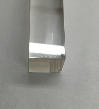
| − | | 01/10/2016 || Pictures || Documentation as arrived at CUA (received from Caltech). Name of the crystal was observed scratched on the face. [[MainPage:Nuclear:NPS:PWO:CrystalLOG: | + | | 01/10/2016 || Pictures || Documentation as arrived at CUA (received from Caltech). Name of the crystal was observed scratched on the face. [[MainPage:Nuclear:NPS:PWO:CrystalLOG:SICCA15#Pictures_at_01.2F10.2F2016|Pictures 01/10/2016]]. |
|- | |- | ||
| 01/14/2016 || Long. Transmittance || Crystal unwrapped. | | 01/14/2016 || Long. Transmittance || Crystal unwrapped. | ||
|- | |- | ||
| + | | 01/14/2016 || Transverse Transmittance || Spectral measurement. | ||
| + | |- | ||
| + | | 06/01/2016 || Longitudinal Transmittance || Spectral measurement, Lambda 950 (integrating sphere). Wrapped crystal. | ||
| + | |- | ||
| + | | 06/02/2016 || Longitudinal Transmittance || Repeating measurement, to make sure alignment and other effects are indeed negligible in our setup. | ||
| + | |- | ||
| + | | 06/03/2016 || Thermal annealing || Ramp up at 18oC/hour up to 200oC. Stays for 10 hours and ramp down at 18oC/hour. | ||
| + | |- | ||
| + | | 06/06/2016 || Transverse Transmittance || Spectral measurement with Lambda 750. | ||
| + | |- | ||
| + | | 06/06/2016 || Transverse Transmittance || Spectral measurement with Lambda 950 - integrated sphere (may not be at exactly the same position). | ||
| + | |- | ||
| + | | 06/06/2016 || Crystal wrapped || 5 layers of teflon tape and 2 layers of black electrical tape. | ||
| + | |- | ||
| + | | 06/06/2016 || Longitudinal Transmittance || Spectral measurement with Lambda 950 - integrated sphere. | ||
| + | |} | ||
| + | |||
| + | == Transmittance measurements == | ||
| + | |||
| + | === Longitudinal transmittance === | ||
| + | |||
| + | {| border="0" style="text-align:center;" width="100%" | ||
| + | |- | ||
| + | | valign="top"| | ||
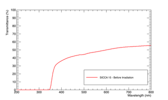
| + | [[File:SICCA 15 LT BI.png|thumb|center|340px|Longitudinal transmittance measured at Lambda 750 (no integrating sphere). Crystal as arrived at CUA (probably irradiated at Caltech).]] | ||
| + | | valign="top"| | ||
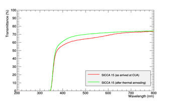
| + | [[File:SICCA15_LT_sphere_anneal.png|thumb|center|340px|Longitudinal transmittance measured at Lambda 950 (with integrating sphere).]] | ||
|} | |} | ||
| Line 29: | Line 56: | ||
|- | |- | ||
| valign="top"| | | valign="top"| | ||
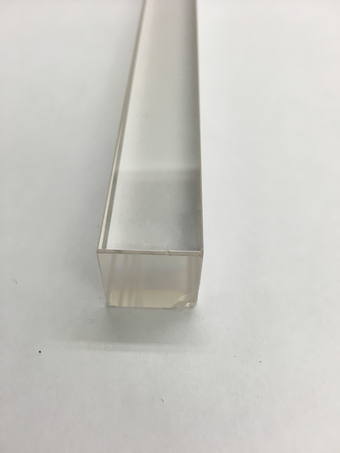
| − | [[File: | + | [[File:Sic15_1.png|thumb|center|340px|Close-up view of crack on edge..]] |
| + | | valign="top"| | ||
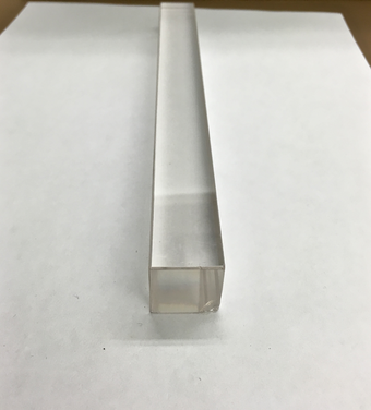
| + | [[File:Sic15_2.png|thumb|center|340px|View of crystal and crack on edge.]] | ||
| + | |- | ||
| + | |} | ||
| + | {| border="0" style="text-align:center;" width="100%" | ||
| + | |- | ||
| valign="top"| | | valign="top"| | ||
| − | [[File: | + | [[File:Sic15_3.png|thumb|center|340px|Carving of "PWO SIC 15" clearly shown on crystal, along with an even closer up view of crack on the edge.]] |
| + | |- | ||
|} | |} | ||
Latest revision as of 15:46, 6 June 2016
| ⇐ Back to Crystal LOG |
| ⇐ Back to Neutral Particle Spectrometer |
| ⇐ Back to the Main_Page |
Time LOG
| Date | Description | Comments |
|---|---|---|
| 01/10/2016 | Pictures | Documentation as arrived at CUA (received from Caltech). Name of the crystal was observed scratched on the face. Pictures 01/10/2016. |
| 01/14/2016 | Long. Transmittance | Crystal unwrapped. |
| 01/14/2016 | Transverse Transmittance | Spectral measurement. |
| 06/01/2016 | Longitudinal Transmittance | Spectral measurement, Lambda 950 (integrating sphere). Wrapped crystal. |
| 06/02/2016 | Longitudinal Transmittance | Repeating measurement, to make sure alignment and other effects are indeed negligible in our setup. |
| 06/03/2016 | Thermal annealing | Ramp up at 18oC/hour up to 200oC. Stays for 10 hours and ramp down at 18oC/hour. |
| 06/06/2016 | Transverse Transmittance | Spectral measurement with Lambda 750. |
| 06/06/2016 | Transverse Transmittance | Spectral measurement with Lambda 950 - integrated sphere (may not be at exactly the same position). |
| 06/06/2016 | Crystal wrapped | 5 layers of teflon tape and 2 layers of black electrical tape. |
| 06/06/2016 | Longitudinal Transmittance | Spectral measurement with Lambda 950 - integrated sphere. |
