Difference between revisions of "MainPage:Nuclear:NPS:PWO:CrystalLOG:SICCAJ41"
Jump to navigation
Jump to search
| (16 intermediate revisions by 3 users not shown) | |||
| Line 30: | Line 30: | ||
| 07/08/2016 || Longitudinal Transmittance Scan || Wavelengths: 200-800 nm. Sampling period: 0.6s, moving motor at 2mm/s. | | 07/08/2016 || Longitudinal Transmittance Scan || Wavelengths: 200-800 nm. Sampling period: 0.6s, moving motor at 2mm/s. | ||
|- | |- | ||
| − | | 07/26/2016 || Light Yield || 3 layers of teflon tape, 1 layer of electrical tape. ~50,000 incidents | + | | 07/26/2016 || Light Yield || Run: 3255. 3 layers of teflon tape, 1 layer of electrical tape. ~50,000 incidents. Light Yield: 13.40011277 pe/MeV |
| + | |- | ||
| + | |07/27/16 || Light Yield || 3 layers of teflon 1 later of electrical. ~50,000 incidents at ~18 degrees Celsius. 200ns gatewidth->900ns | ||
| + | gatewidth. | ||
| + | 200ns: 3321, 300ns:3322, 400ns:3323, 500ns:3324, 600ns:3325, 700ns:3328, 800ns:3329, 900ns:3330 | ||
| + | |- | ||
| + | | 07/07/2017 || Longitudinal Transmittance Scan || Wavelengths: 200-800 nm. Sampling period: 0.6s, moving motor at 2mm/s. | ||
| + | |- | ||
| + | | 07/10/2017 || Light Yield || Run 3694. 100ns gw. ~50,000 incidents ~3 layers of teflon tape ~1 layer of electrical. LY=7.509 pe/MeV. | ||
| + | |- | ||
| + | | 08/01/2017 || Summer Students || Transverse Transmittance Scan --Wavelengths: 200-800 nm. 10cm down. | ||
| + | |- | ||
| + | | 08/01/2017 || Summer Students || Xray Radiation 70 minutes, 160mV, 6mA. ___ mm from beam origin. Wait time to transmittance measurement ~2 minutes... not constant.dk= 0.8562 | ||
| + | |- | ||
| + | | 08/02/2017 || Summer Students || Transverse Transmittance Scan Wavelengths: 200-800 nm. 10cm down. | ||
| + | |- | ||
| + | | 08/02/2017 || Summer Students || LED curing 34 LEDs, 3.5 V for 7 minutes. | ||
| + | |- | ||
| + | | 08/02/2017 || Summer Students || Transverse Transmittance Scan-- Wavelengths: 200-800 nm. 10cm down. | ||
| + | |- | ||
| + | | 08/02/2017 || Summer Students || LED curing 34 LEDs, 3.5 V for 7 more minutes (14 total). | ||
| + | |- | ||
| + | | 08/02/2017 || Summer Students || Transverse Transmittance Scan-- Wavelengths: 200-800 nm. 10cm down. | ||
| + | |- | ||
| + | | 08/02/2017 || Summer Students || LED curing-- 34 LEDs, 3.5 V for 7 more minutes (21 total). | ||
| + | |- | ||
| + | | 08/02/2017 || Summer Students || Transverse Transmittance Scan--Wavelengths: 200-800 nm. 10cm down. | ||
| + | |||
|} | |} | ||
| Line 41: | Line 68: | ||
| valign="top"| | | valign="top"| | ||
[[File:SICCAJ41.JPG|thumb|center|340px|xxxx.]] | [[File:SICCAJ41.JPG|thumb|center|340px|xxxx.]] | ||
| + | |} | ||
| + | |||
| + | == Light Yield == | ||
| + | {|border="0" style="text-align:center;" width="100%" | ||
| + | |- | ||
| + | | valign="top"| | ||
| + | [[File:J41-100nsgw.png|thumb|left|340px| 07/26/2016]] | ||
| + | |} | ||
| + | |||
| + | == Light Yield Gate Width== | ||
| + | {|border="0" style="text-align:center;" width="100%" | ||
| + | |- | ||
| + | | valign="top"| | ||
| + | [[File:J41-100-900 gw.png|thumb|left|340px| 07/27/2016]] | ||
| + | |||
| + | ==Radiation Hardness== | ||
| + | {|border="0" style="text-align:center;" width="100%" | ||
| + | |- | ||
| + | | valign="right"| | ||
| + | [[File:J41IR.png|thumb|left|340px| 08/02/2017.dk= 0.8520606]] | ||
| + | |} | ||
| + | |||
| + | == LED Curing== | ||
| + | {|border="0" style="text-align:center;" width="100%" | ||
| + | |- | ||
| + | | valign="top"| | ||
| + | [[File:J41LED.png|thumb|left|340px| 08/02/2017]] | ||
|} | |} | ||
Latest revision as of 09:14, 3 August 2017
| ⇐ Back to Crystal LOG |
| ⇐ Back to Neutral Particle Spectrometer |
| ⇐ Back to the Main_Page |
Time LOG
| Date | Description | Comments |
|---|---|---|
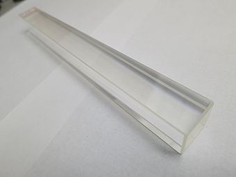
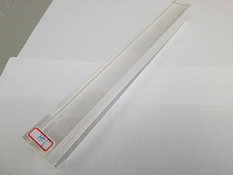
| 04/29/2016 | Pictures | Documentation of crystal's conditions as it arrived at CUA. |
| 04/29/2016 | Thermal annealing | Ramp up at 18oC/hour up to 200oC. Stays for 10 hours and ramp down at 18oC/hour. |
| 05/19/2016 | Transverse Transmittance | At the center of the crystal, every nm from 200nm until 800nm. Sample: 1355 |
| 05/20/2016 | Light Yield | Run 3216: crystal wrapped with ~5 layers of teflon tape and 2 layers of black electrical tape. Steps of 20min, 1cm. T=18°C. LY = 12.53 ± 0.672 pe/MeV. |
| 05/20/2016 | Transverse Transmittance Scan | Wavelengths: 360nm, 420nm, 620nm. Sampling period: 0.6s, moving motor at 2mm/s. |
| 07/08/2016 | Longitudinal Transmittance Scan | Wavelengths: 200-800 nm. Sampling period: 0.6s, moving motor at 2mm/s. |
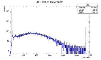
| 07/26/2016 | Light Yield | Run: 3255. 3 layers of teflon tape, 1 layer of electrical tape. ~50,000 incidents. Light Yield: 13.40011277 pe/MeV |
| 07/27/16 | Light Yield | 3 layers of teflon 1 later of electrical. ~50,000 incidents at ~18 degrees Celsius. 200ns gatewidth->900ns
gatewidth. 200ns: 3321, 300ns:3322, 400ns:3323, 500ns:3324, 600ns:3325, 700ns:3328, 800ns:3329, 900ns:3330 |
| 07/07/2017 | Longitudinal Transmittance Scan | Wavelengths: 200-800 nm. Sampling period: 0.6s, moving motor at 2mm/s. |
| 07/10/2017 | Light Yield | Run 3694. 100ns gw. ~50,000 incidents ~3 layers of teflon tape ~1 layer of electrical. LY=7.509 pe/MeV. |
| 08/01/2017 | Summer Students | Transverse Transmittance Scan --Wavelengths: 200-800 nm. 10cm down. |
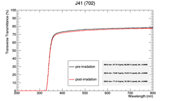
| 08/01/2017 | Summer Students | Xray Radiation 70 minutes, 160mV, 6mA. ___ mm from beam origin. Wait time to transmittance measurement ~2 minutes... not constant.dk= 0.8562 |
| 08/02/2017 | Summer Students | Transverse Transmittance Scan Wavelengths: 200-800 nm. 10cm down. |
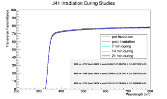
| 08/02/2017 | Summer Students | LED curing 34 LEDs, 3.5 V for 7 minutes. |
| 08/02/2017 | Summer Students | Transverse Transmittance Scan-- Wavelengths: 200-800 nm. 10cm down. |
| 08/02/2017 | Summer Students | LED curing 34 LEDs, 3.5 V for 7 more minutes (14 total). |
| 08/02/2017 | Summer Students | Transverse Transmittance Scan-- Wavelengths: 200-800 nm. 10cm down. |
| 08/02/2017 | Summer Students | LED curing-- 34 LEDs, 3.5 V for 7 more minutes (21 total). |
| 08/02/2017 | Summer Students | Transverse Transmittance Scan--Wavelengths: 200-800 nm. 10cm down. |
Pictures at 04/29/2016
Light Yield
Light Yield Gate Width
|
File:J41-100-900 gw.png 07/27/2016 Radiation HardnessLED Curing |
