Difference between revisions of "MainPage:Nuclear:NPS:PWO:CrystalLOG:SICCAJ16"
Jump to navigation
Jump to search
| Line 14: | Line 14: | ||
</b></font> | </b></font> | ||
| − | ! "background:#f5f5f5;" style="text-align:center; background:lavender; font-weight:bold; width:10%;" | Date | + | ! "background:#f5f5f5;" style="text-align:center; background:lavender; font-weight:bold; width:10%;" | Date |
| + | ! "background:#f5f5f5;" style="text-align:center; background:lavender; font-weight:bold; width:15%;" | Experimenter | ||
! "background:#f5f5f5;" style="text-align:center; background:lavender; font-weight:bold; width:15%;" | Description | ! "background:#f5f5f5;" style="text-align:center; background:lavender; font-weight:bold; width:15%;" | Description | ||
! "background:#f5f5f5;" style="text-align:center; background:lavender; font-weight:bold; width:75%;" | Comments | ! "background:#f5f5f5;" style="text-align:center; background:lavender; font-weight:bold; width:75%;" | Comments | ||
|- | |- | ||
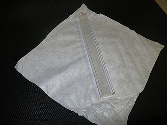
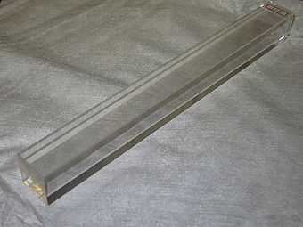
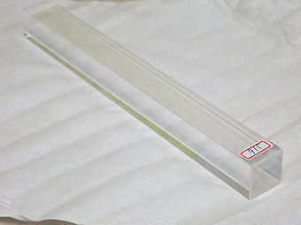
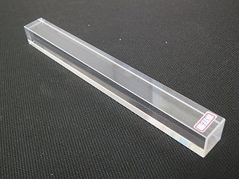
| − | | 12/14/2015 || Pictures || Documentation of crystal's conditions as it arrived at CUA. | + | | 12/14/2015 || Marco || Pictures || Documentation of crystal's conditions as it arrived at CUA. |
|- | |- | ||
| − | | 12/14/2015 || Wrapped || Preparing for light yield measurement. Approximately 5 layers of teflon tape, and 2 layers of black tape. | + | | 12/14/2015 || Marco || Wrapped || Preparing for light yield measurement. Approximately 5 layers of teflon tape, and 2 layers of black tape. |
|- | |- | ||
| − | | 12/15/2015 || LY scan || Measurement of LY along crystal. More details in the LOGBOOK, runs xx.. | + | | 12/15/2015 || Marco || LY scan || Measurement of LY along crystal. More details in the LOGBOOK, runs xx.. |
|- | |- | ||
| − | | 02/01/2016 || Thermal annealing || Ramp up at 18oC/hour up to 200oC. Stays for 10 hours and ramp down at 18oC/hour. | + | | 02/01/2016 || Marco || Thermal annealing || Ramp up at 18oC/hour up to 200oC. Stays for 10 hours and ramp down at 18oC/hour. |
|- | |- | ||
| − | | 03/04/2016 || Transverse Transmittance || At the center of the crystal, every nm from 200nm until 800nm. Sample: 1317 | + | | 03/04/2016 || Marco || Transverse Transmittance || At the center of the crystal, every nm from 200nm until 800nm. Sample: 1317 |
|- | |- | ||
| − | | 03/04/2016 || Dimensions || Crystal's dimensions measured. Length and six points of width (3 in each face). | + | | 03/04/2016 || Marco || Dimensions || Crystal's dimensions measured. Length and six points of width (3 in each face). |
|- | |- | ||
| − | | 05/23/2016 || Transverse Transmittance Scan || Wavelengths: 360nm, 420nm, 620nm. Sampling period: 0.6s, moving motor at 2mm/s. | + | | 05/23/2016 || Marco || Transverse Transmittance Scan || Wavelengths: 360nm, 420nm, 620nm. Sampling period: 0.6s, moving motor at 2mm/s. |
|- | |- | ||
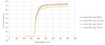
| − | | 07/05/2016 || Longitudinal Transmittance Scan || Wavelengths: 200-800nm. Measured effect of iris diameter on transmittance. 8.0mm, 11.5mm, 15mm, and 17mm. | + | | 07/05/2016 || Marco || Longitudinal Transmittance Scan || Wavelengths: 200-800nm. Measured effect of iris diameter on transmittance. 8.0mm, 11.5mm, 15mm, and 17mm. |
|- | |- | ||
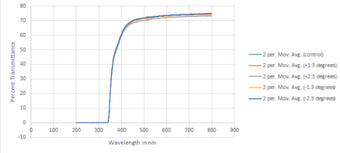
| − | | 07/14/2016 || Longitudinal Transmittance Scan || Wavelengths: 200-800nm. Measured effect of off center crystal placement on transmittance. +1.3°C, +2.3°C, -1.3°C, -2.3°C. | + | | 07/14/2016 || Marco || Longitudinal Transmittance Scan || Wavelengths: 200-800nm. Measured effect of off center crystal placement on transmittance. +1.3°C, +2.3°C, -1.3°C, -2.3°C. |
|- | |- | ||
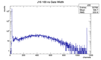
| − | | 07/26/2016 || Light Yield || Run 3250. 100ns gw. ~50,000 incidents ~3 layers of teflon tape ~1 layer of electrical. | + | | 07/26/2016 || Marco || Light Yield || Run 3250. 100ns gw. ~50,000 incidents ~3 layers of teflon tape ~1 layer of electrical. |
|- | |- | ||
| − | |07/29/2016 || Transverse Transmittance || At 10cm. 200-800nm wavelength. | + | |07/29/2016 || Marco || Transverse Transmittance || At 10cm. 200-800nm wavelength. |
|- | |- | ||
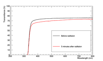
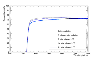
| − | | 07/29/16 || X-Ray Irradiation || 160kV 6.3mA 70 minutes. 14.16 cm for LabJack on shelf 8. 6290R/min ionization rate. | + | | 07/29/16 || Marco || X-Ray Irradiation || 160kV 6.3mA 70 minutes. 14.16 cm for LabJack on shelf 8. 6290R/min ionization rate. |
|- | |- | ||
| − | |07/29/2016 || Transverse Transmittance || At 10cm. 200-800nm wavelength. | + | |07/29/2016 || Marco || Transverse Transmittance || At 10cm. 200-800nm wavelength. |
|- | |- | ||
| − | |07/29/2016 || LED curing || 7 minutes with 34 blue LEDs. 3.5 V. Millipore cover placed over lights and crystal. | + | |07/29/2016 || Marco || LED curing || 7 minutes with 34 blue LEDs. 3.5 V. Millipore cover placed over lights and crystal. |
|- | |- | ||
| − | |07/29/2016 || Transverse Transmittance || At 10cm. 200-800nm wavelength. | + | |07/29/2016 || Marco || Transverse Transmittance || At 10cm. 200-800nm wavelength. |
|- | |- | ||
| − | |07/29/2016 || LED curing || 7 more minutes (14 minutes total) with 34 blue LEDs. 3.5 V. Millipore cover placed over lights and crystal. | + | |07/29/2016 || Marco || LED curing || 7 more minutes (14 minutes total) with 34 blue LEDs. 3.5 V. Millipore cover placed over lights and crystal. |
|- | |- | ||
| − | |07/29/2016 || Transverse Transmittance || At 10cm. 200-800nm wavelength. | + | |07/29/2016 || Marco || Transverse Transmittance || At 10cm. 200-800nm wavelength. |
|- | |- | ||
| − | |07/29/2016 || LED curing || 7 more minutes (21 minutes total) with 34 blue LEDs. 3.5 V. Millipore cover placed over lights and crystal. | + | |07/29/2016 || Marco || LED curing || 7 more minutes (21 minutes total) with 34 blue LEDs. 3.5 V. Millipore cover placed over lights and crystal. |
|} | |} | ||
Revision as of 20:15, 30 November 2016
| ⇐ Back to Crystal LOG |
| ⇐ Back to Neutral Particle Spectrometer |
| ⇐ Back to the Main_Page |
Time LOG
| Date | Experimenter | Description | Comments |
|---|---|---|---|
| 12/14/2015 | Marco | Pictures | Documentation of crystal's conditions as it arrived at CUA. |
| 12/14/2015 | Marco | Wrapped | Preparing for light yield measurement. Approximately 5 layers of teflon tape, and 2 layers of black tape. |
| 12/15/2015 | Marco | LY scan | Measurement of LY along crystal. More details in the LOGBOOK, runs xx.. |
| 02/01/2016 | Marco | Thermal annealing | Ramp up at 18oC/hour up to 200oC. Stays for 10 hours and ramp down at 18oC/hour. |
| 03/04/2016 | Marco | Transverse Transmittance | At the center of the crystal, every nm from 200nm until 800nm. Sample: 1317 |
| 03/04/2016 | Marco | Dimensions | Crystal's dimensions measured. Length and six points of width (3 in each face). |
| 05/23/2016 | Marco | Transverse Transmittance Scan | Wavelengths: 360nm, 420nm, 620nm. Sampling period: 0.6s, moving motor at 2mm/s. |
| 07/05/2016 | Marco | Longitudinal Transmittance Scan | Wavelengths: 200-800nm. Measured effect of iris diameter on transmittance. 8.0mm, 11.5mm, 15mm, and 17mm. |
| 07/14/2016 | Marco | Longitudinal Transmittance Scan | Wavelengths: 200-800nm. Measured effect of off center crystal placement on transmittance. +1.3°C, +2.3°C, -1.3°C, -2.3°C. |
| 07/26/2016 | Marco | Light Yield | Run 3250. 100ns gw. ~50,000 incidents ~3 layers of teflon tape ~1 layer of electrical. |
| 07/29/2016 | Marco | Transverse Transmittance | At 10cm. 200-800nm wavelength. |
| 07/29/16 | Marco | X-Ray Irradiation | 160kV 6.3mA 70 minutes. 14.16 cm for LabJack on shelf 8. 6290R/min ionization rate. |
| 07/29/2016 | Marco | Transverse Transmittance | At 10cm. 200-800nm wavelength. |
| 07/29/2016 | Marco | LED curing | 7 minutes with 34 blue LEDs. 3.5 V. Millipore cover placed over lights and crystal. |
| 07/29/2016 | Marco | Transverse Transmittance | At 10cm. 200-800nm wavelength. |
| 07/29/2016 | Marco | LED curing | 7 more minutes (14 minutes total) with 34 blue LEDs. 3.5 V. Millipore cover placed over lights and crystal. |
| 07/29/2016 | Marco | Transverse Transmittance | At 10cm. 200-800nm wavelength. |
| 07/29/2016 | Marco | LED curing | 7 more minutes (21 minutes total) with 34 blue LEDs. 3.5 V. Millipore cover placed over lights and crystal. |
