Difference between revisions of "MainPage:Nuclear:NPS:PWO:CrystalLOG:SICCAJ30"
Jump to navigation
Jump to search
| Line 52: | Line 52: | ||
| valign="top"| | | valign="top"| | ||
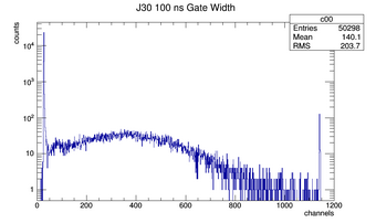
[[File:J30-100nsgw.png|thumb|left|340px| 07/21/2016]] | [[File:J30-100nsgw.png|thumb|left|340px| 07/21/2016]] | ||
| + | | valign="top"| | ||
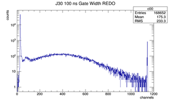
| + | [[File:J30-100nsgwREDO.png|thumb|left|340px| 08/01/2016]] | ||
| + | |||
|} | |} | ||
Revision as of 14:42, 11 August 2016
| ⇐ Back to Crystal LOG |
| ⇐ Back to Neutral Particle Spectrometer |
| ⇐ Back to the Main_Page |
Time LOG
| Date | Description | Comments |
|---|---|---|
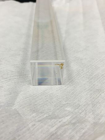
| 03/09/2016 | Pictures | Documentation of crystal's conditions as it arrived at CUA. |
| 03/09/2016 | Dimensions | Crystal's dimensions measured. Length and six points of width (3 in each face). |
| 03/18/2016 | Thermal annealing | Ramp up at 18oC/hour up to 200oC. Stays for 10 hours and ramp down at 18oC/hour. |
| 04/13/2016 | Light Yield | Run 3171: crystal wrapped with ~5 layers of teflon tape and 2 layers of black tape. Steps of 20min, 1cm. T=18oC. LY = 14.95 pe/MeV. |
| 05/17/2016 | Transverse Transmittance | At the center of the crystal, every nm from 200nm until 800nm. Sample: 1341 |
| 05/20/2016 | Transverse Transmittance Scan | Wavelengths: 360nm, 420nm, 620nm. Sampling period: 0.6s, moving motor at 2mm/s. |
| 07/06/2016 | Longitudinal Transmittance Scan | Wavelengths: 200-800 nm. Sampling period: 0.6s, moving motor at 2mm/s. |
| 07/23/2016 | Light Yield | Run:3236 ~3layers of teflon tape and 1 layer of black tape. ~50,000 incidents recorded at ~18 degrees Celsius. |
| 08/01/2016 | Transverse Transmittance Scan | All wavelenghts, 10cm down the crystal. |
| 08/11/2016 | Light Yield | Run:3409 ~3layers of teflon tape and 1 layer of black tape. ~50,000 incidents recorded at ~18 degrees Celsius. LY: 12.18 |


