Difference between revisions of "MainPage:Nuclear:NPS:PWO:CrystalLOG:SICCA5201"
Jump to navigation
Jump to search
(Created page with "{|border="1" cellpadding="2" cellspacing="0" style="background-color:lightgray" | <font size="2">'''⇐ Back to Crystal LOG'''</font> |...") |
|||
| Line 19: | Line 19: | ||
! "background:#f5f5f5;" style="text-align:center; background:lavender; font-weight:bold; width:75%;" | Comments | ! "background:#f5f5f5;" style="text-align:center; background:lavender; font-weight:bold; width:75%;" | Comments | ||
|- | |- | ||
| − | | 11/ | + | | 11/8/2017 || Arshak || Visual Inspection || Documentation of crystal's conditions as it arrived at JLab. |
|- | |- | ||
| − | | 11/ | + | | 11/15/2017 || Tanja || Visual Inspection || Documentation of crystal's conditions as it arrived at CUA. |
|- | |- | ||
| 11/XX/2017 || Tanja || Thermal annealing || Ramp up at 18oC/hour up to 200oC. Stay for 10 hours and ramp down at 18oC/hour. | | 11/XX/2017 || Tanja || Thermal annealing || Ramp up at 18oC/hour up to 200oC. Stay for 10 hours and ramp down at 18oC/hour. | ||
| Line 32: | Line 32: | ||
|- | |- | ||
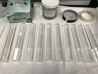
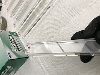
| − | == Pictures 11/ | + | == Pictures 11/15/2017 == |
{| border="0" style="text-align:center;" width="100%" | {| border="0" style="text-align:center;" width="100%" | ||
|- | |- | ||
| valign="top"| | | valign="top"| | ||
| − | [[File: | + | [[File:IMG 0361.JPG|thumb|center|340px|xxxx.]] |
| valign="top"| | | valign="top"| | ||
| − | [[File:IMG .JPG|thumb|center|340px|xxxx.]] | + | [[File:IMG 0362.JPG|thumb|center|340px|xxxx.]] |
|- | |- | ||
| valign="top"| | | valign="top"| | ||
[[File:IMG .JPG|thumb|center|340px|xxxx.]] | [[File:IMG .JPG|thumb|center|340px|xxxx.]] | ||
| valign="top"| | | valign="top"| | ||
| − | [[File: | + | [[File:PWO-SICCAS-box2-5-6.png|thumb|center|340px|xxxx.]] |
|} | |} | ||
Latest revision as of 18:45, 15 November 2017
| ⇐ Back to Crystal LOG |
| ⇐ Back to Neutral Particle Spectrometer |
| ⇐ Back to the Main_Page |
Time LOG
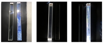
Pictures 11/15/2017
| Date | Experimenter | Description | Comments |
|---|---|---|---|
| 11/8/2017 | Arshak | Visual Inspection | Documentation of crystal's conditions as it arrived at JLab. |
| 11/15/2017 | Tanja | Visual Inspection | Documentation of crystal's conditions as it arrived at CUA. |
| 11/XX/2017 | Tanja | Thermal annealing | Ramp up at 18oC/hour up to 200oC. Stay for 10 hours and ramp down at 18oC/hour. |
| 11/XX/2017 | Tanja | Longitudinal Transmittance Scan | Wavelengths: 200-800nm. |
| 11/X/2017 | Tanja | Wrapped | Preparing for light yield measurement. 3 layers of teflon tape, and 2 layers of black tape. |
| 11/XX/2017 | Tanja | LY scan | Measurement of LY along crystal. More details in the LOGBOOK, runs xx.. |
|
File:IMG .JPG xxxx. |
Longitudinal and Transverse Transmittance (TT)
Light Yield
|
File:5201-100nsgw.png 11/XX/2017 |
Radiation Hardness
|
File:5201 radiation hardness.png XX/XX/XXXX. Wait time to transmittance measurement ~15 minutes. |


