Difference between revisions of "MainPage:Nuclear:NPS:PWO:CrystalLOG:SICCAJ45"
Jump to navigation
Jump to search
| Line 25: | Line 25: | ||
|- | |- | ||
| 05/20/2016 || Transverse Transmittance Scan || Wavelengths: 360nm, 420nm, 620nm. Sampling period: 0.6s, moving motor at 2mm/s. | | 05/20/2016 || Transverse Transmittance Scan || Wavelengths: 360nm, 420nm, 620nm. Sampling period: 0.6s, moving motor at 2mm/s. | ||
| + | |- | ||
| + | | 05/25/2016 || Light Yield || Run 3220: crystal wrapped with ~5 layers of teflon tape and 2 layers of black electrical tape. Steps of 20min, 1cm. T=18°C. LY = 15.38 ± 0.612 pe/MeV. | ||
|} | |} | ||
Revision as of 13:13, 2 June 2016
| ⇐ Back to Crystal LOG |
| ⇐ Back to Neutral Particle Spectrometer |
| ⇐ Back to the Main_Page |
Time LOG
| Date | Description | Comments |
|---|---|---|
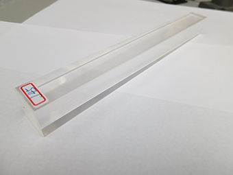
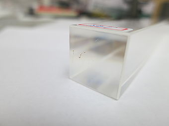
| 05/02/2016 | Pictures | Documentation of crystal's conditions as it arrived at CUA. |
| 05/02/2016 | Thermal annealing | Ramp up at 18oC/hour up to 200oC. Stays for 10 hours and ramp down at 18oC/hour. |
| 05/19/2016 | Transverse Transmittance | At the center of the crystal, every nm from 200nm until 800nm. Sample: 1362 |
| 05/20/2016 | Transverse Transmittance Scan | Wavelengths: 360nm, 420nm, 620nm. Sampling period: 0.6s, moving motor at 2mm/s. |
| 05/25/2016 | Light Yield | Run 3220: crystal wrapped with ~5 layers of teflon tape and 2 layers of black electrical tape. Steps of 20min, 1cm. T=18°C. LY = 15.38 ± 0.612 pe/MeV. |

